Anisotropic Etching - Bulk plasma etching provided • Ashing plasma sources available
Plasma etching is a vital production tool used by the semiconductor manufacturing industry for microfabrication. During the early days of printed circuit board (PCB) manufacturing, wet etching processes were employed to remove photoresist material from PCBs. This process is called “wet” because it utilizes liquid acids as chemical reagents to remove unwanted surface material not protected by masking.
Wet etching is a relatively simple process used to remove material in a general area by immersing the silicon wafer in a liquid etchant bath were a chemical reaction takes place, removing unprotected material. Wet etching is generally isotropic – that is, it removes material equally in every direction. However, it can also be anisotropic -- removing material in one direction -- such as needed for creating circuitry patterns. However, the major disadvantage of wet chemical etching for pattern transfer is the undercutting of the layer underneath the mask, resulting in a loss of resolution in the etched pattern. More often than not, wet etching is utilized for isotropic processes, such as cleaning substrates and wafers.
There are several drawbacks to both anisotropic and isotropic wet etching, including safety and sanitary hazards resulting from the use of harmful pollutants such as hydrofluoric acid, high defect levels due to solution particulate contamination, and poor repeatability.
Anisotropic and isotropic plasma etching
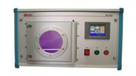
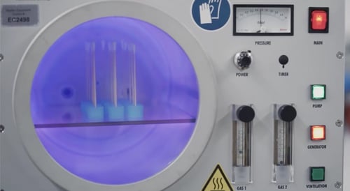
Plasma etching and cleaning technologies are widely used in the semiconductor and integrated circuit manufacturing industry. Plasma etching is also referred to as dry etching because it is performed in a gas phase without the use of liquids. It is sometimes referred to as reactive ion etching (RIE), although the correct term should be ion-assisted chemical vapor etching. In plasma etching systems, the substrate is placed in a vacuum chamber and gases are introduced to produce the reaction.
 Like wet etching, dry plasma etching can be used for both isotropic and anisotropic etching. Major benefits of using plasma technology for either type, though, include a more environmentally-friendly process, no toxic by-products, reliable repeatability, lower defect rates, and greater efficiency.
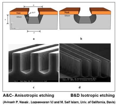
Dry plasma etching is one of the most common pattern transfer techniques used in IC manufacturing, hence its popularity for use in anisotropic processes. In contrast to isotropic etching, which produces a lower resolution concave shape under the photoresist etching mask, anisotropic etching removes material in specific directions enabling the production of geometric characteristics such as sharp corners, flat surfaces, and deep cavities. A patterned resist layer acts as a mask for an underlying substrate such as silicon during the etching process. Plasma etching is widely used for etching nanoscale features because it can produce vertical sidewall profiles with little or no undercut. Another aspect that makes plasma etching suitable for small features is the ability of gas species to diffuse into smaller features better than liquids. Plasma etching is also highly repeatable compared to wet etching liquid bath.
As microelectronic circuits has gotten smaller, denser, and more complex, the IC manufacturing industry has turned increasingly to plasma technology to address evolving etching challenges.
To learn more about etching, check out our eBook titled "Plasma Etching and Cleaning Strategy for Better Product Quality."