Plasma Treatment Articles
Plasma Activation,
Plasma Treatment
|
4 min read
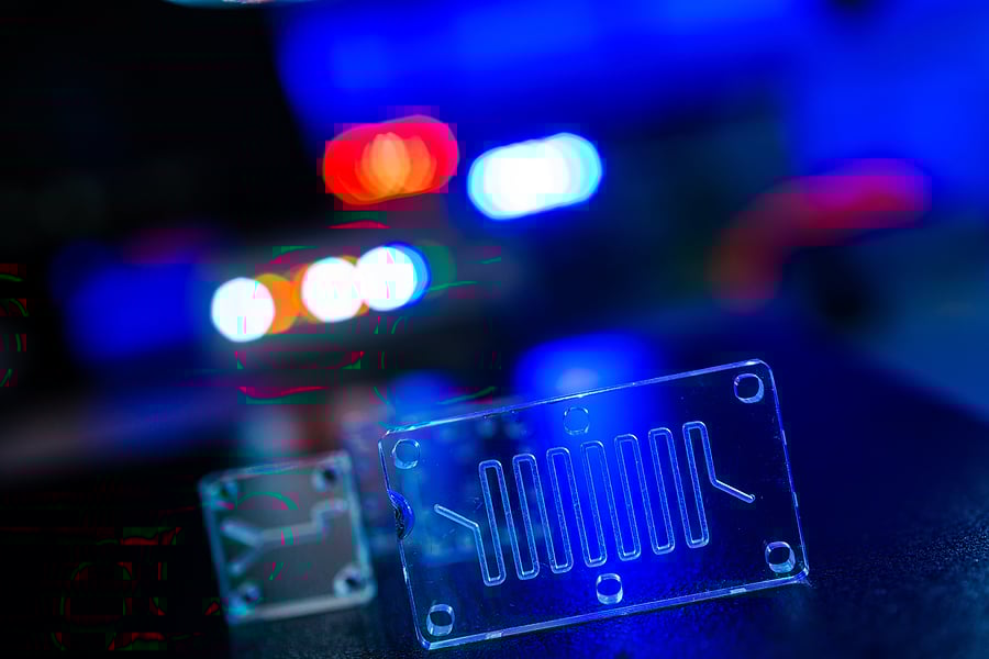
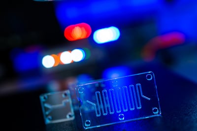
In present-day microfluidic device manufacturing, producing good adhesion between PDMS and the silicon-containing mating surface is performed by plasma activation. This plasma activation of the microfluidic silicon-containing parts is the key process that enables covalent bonding without a traditional adhesive. Plasma activation can be performed to produce a bond at some low level of relative adhesion, or it can be optimized to a higher level of repeatable bond strength that provides an increased level of device performance and reliability. This subtle difference in plasma process optimization and control leads to increased adhesion and superior microfluidic device performance.
Choosing a plasma system designed for microfluidic device activation with the proper control, instrumentation, design, material selection, and process optimization is key to achieving the highest bond strength possible to produce the best performing microfluidic device.
 Often at the early stages of microfluidic device design, the PDMS bond strength requirement is not well defined. For example, the microfluidic device could be used as a teaching aid with low bond strength requirements, a fluid handling assay tray with moderate bond strength requirements, or a high-pressure fluid handling instrument with very high bond strength requirements. Some of the considerations to determine the level of plasma activation required in your microfluidic device could be bond strength, the cost of a device failure, and the time involved to produce your device. The lowest-cost plasma activation tool that can bond PDMS is often not the most cost-effective solution to the manufacturing requirements and product requirements at hand. Variation in plasma activation and process control can lead to product failures and scrap, leading to low customer satisfaction and increased device production cost.
A significant factor in controlling plasma activation of microfluidic devices is accurate pressure control during the plasma process. Precise pressure control of the process gas determines the concentration of oxygen plasma coming into contact with the PDMS surface and mating silicon-containing parts. This plasma process pressure control is performed by having an automatic process control loop between the pressure measurement instrumentation and the mass flow control valve controlling the gas flow into the vacuum chamber. This controlled injection of gas into the vacuum chamber is continuously adjusted. as the vacuum pump removes gas from the vacuum chamber to produce the desired process pressure. Plasma systems designed for plasma activation of microfluidic device components have careful consideration of process pressure control designed explicitly for activating PDMS. Fluctuation in plasma activation process pressure will result in fluctuations in the bond strength and burst pressure of the finished microfluidic devices.
 Management of the gas settling time is also an essential factor for optimized plasma activation. Gas settling time is the amount of time that process gas flows in the vacuum chamber after the pump down pressure is reached and before the plasma activation process starts. When we begin to flow gas into the process chamber, process gas will be a mixture of the residual air in the chamber and the process gas introduced into the chamber. By accurately controlling the settling time, the process will not start until the process gas is at a known concentration in the vacuum chamber. This known concentration of process gas provides an accurate rate of plasma activation on the PDMS surface and silicon containing mating part. Suppose there is no precise control of the gas settling. In that case, variation can occur in the early stages of the plasma process activation, causing non-uniformity in the PDMS activation leading to non-uniform device burst pressure.
The total time the PDMS and silicon-containing mating part are in the plasma determine the level of activation on the parts' surface. This optimized level of plasma activation leads to the optimized level of covalent bond strength. If the parts are not activated long enough, the activation energy is low, and the bond strength is low. If the parts are plasma-activated too long, the parts' surface will begin to etch, and the bond strength will be low. A narrow process window of activation time must be performed to optimize the covalent bond strength in plasma-activated PDMS and silicon-containing mating parts. Repeatedly controlling the plasm activation process time allows optimization and activation without beginning to etch the PDMS surface or its mating part. Accurate plasma activation process time provides an optimum and uniform bond in microfluidic devices.
Another thing required to turn this carefully controlled gas process into plasma is power. Power control during the plasma process allows the control of what percentage of the gas is in a plasma state and is chemically active in the plasma processing chamber. This percentage of chemically active gas in the plasma process is referred to as plasma disassociation efficiency. The plasma disassociation efficiency will determine the concentration of reactive oxygen plasma species in the chamber. This chemical activity rate will determine the chemical reaction at the PDMS surface and silicon-containing parts causing activation. If the power is too low, there will not be enough chemical reaction, and activation will be low. If the power is too high, the activation process will lead to etching and non-uniformity issues. When this concentration is correct for the proper amount of time, good surface energy and bond strength will be produced in your microfluidic device.
 Producing uniform plasma inside a vacuum chamber of carefully controlled gas does not happen by accident. It is the result of a properly designed electrode to couple power into the plasma chamber. Many manufacturers will wrap a low-cost wire around a chamber as their conductive electrode. This method of coupling RF energy into the plasma chamber produces non-uniform plasma. This non-uniform plasma will lead to variation in plasma activation on the PDMS surface and the silicon-containing mating part. It is essential to have a properly designed electrode for uniform plasma so that all surfaces receive the same, even plasma treatment.
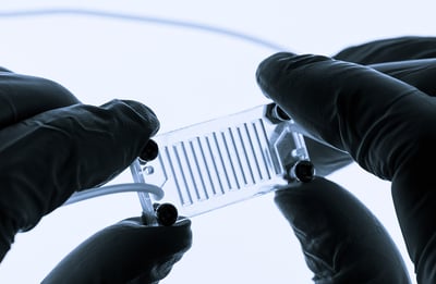
After the plasma activation of the PDMS and the silicon-containing mating part, the plasma chamber is vented. It is best to bond the samples as soon as possible after venting. The activated parts surfaces should contact without any deformation of the material or lateral motion of the parts relative to each other when touching. Often tooling is utilized for alignment and control of the bonding process. Attempting to peel a sample apart for realignment will not result in a bond. After alignment and bonding is performed, it is recommended to allow the devices to continue to bond for approximately 24 hours before testing. This additional time will increase the bond strength and burst pressure of the finished device.
As discussed in this article, accurate and repeatable plasma process controls are crucial to creating reliable plasma-activated PDMS parts for microfluidic device assembly. Carefully controlled plasma activation processes result in the optimization of bond strength and burst pressure in finished microfluidic devices. Identifying plasma systems with the correct capabilities to control these process parameters are important when selecting a plasma system for PDMS bonding and microfluidic device manufacturing.
To learn more about the best practices for plasma activation of microfluidic devices, please read our eBook titled "How to Improve Burst Pressure and Yield in Microfluidic Devices."


Comments