
Etching and cleaning many of today’s modern manufactured surfaces such as silicon wafers can present a host of problems to the manufacturer. Many wet etching processes utilize corrosive and dangerous liquids such as ammonium bisulfate and hydrofluoric acid that can present a hazard to the user and the environment.
Less toxic methods, such as mechanical tumbling and sandblasting take longer and can be less precise and are better suited to creating a macro etch – less useful when electronic components require smaller, more complex circuitry. Photo-ablating uses high energy lasers to create micro etches but the process is restricted to highly localized, smaller areas and is difficult to use for treating entire surfaces. Add to that the significant training and personal protective equipment needed and the process quickly becomes too costly and cumbersome to employ at scale.
Likewise, cleaning processes can present a number of challenges to manufacturers and the results can be underwhelming. For example, common solvents can remove some contaminants but not all and they often leave a residue that can compromise performance. Solvents are prone to simply smearing contaminants around the surface instead of completely removing them and once the solvent has evaporated, there are still trace contaminants remaining that result in a dirty surface despite the best efforts made.
And a dirty surface is not the only problem. There is often a molecular level of contamination left over which will inhibit proper adhesion. A surface must be completely clean, including the removal of molecular level contaminants, to create the pristine surface needed for optimal bonding. Even if the best combination of material and adhesive has been chosen to promote optimal bonding, a dirty surface will result in a poor bond and poor product quality.
Unfortunately, many manufacturers cannot determine if their materials are completely clean. Many manufacturing processes are inherently dirty and leave oils or residues on the surface without the manufacturer even being aware of the issue. Compounding the problem are the waste byproducts created in fluid-driven cleaning processes that are environmentally toxic and harmful if not disposed of properly. While there is a growing push to create greener products and cleaner liquid solvents, toxicity remains an issue and the electronics industry needs to speed the evolution of less toxic processes and cleaner technologies.
 The fallout created by less-than-optimal etching and cleaning processes can be widespread. Poor cleaning or etching methodologies can result in higher product costs caused by additional scrap and added cleaning or etching material expense during production. It also creates considerable waste requiring disposal, which also adds to increased production costs. When product quality suffers because of a poor cleaning or etching process, it can slow down the manufacturing line, creating an additional negative effect on the bottom line. The goal for these cleaning and etching processes should be to make manufacturing more efficient without adding production lines, man hours, or material costs.
Plasma treatment for cleaning and etching enables new manufacturing process and products that would otherwise not be possible, enabling companies to expand their product lines and establish new markets. For example, plasma enhances surface functionalization such as adding carboxyl groups for the medical industry.
Plasma also enables uniform shifts of surface energy over large areas for the coating and bonding industry which requires cleaning and etching first. Semiconductor and wafer production also have a growing need for plasma etching and cleaning applications. Likewise, solar cell manufacturing is ideal for the adoption and increased use of plasma systems due to their ability to accommodate precisely controlled plasma parameters.
Complacency presents a challenge that many companies find difficult to overcome – it’s easy to do nothing. For manufacturers that lack resources or capital, the answer is often to simply produce lower quality parts with an allowable level of contamination that is acceptable for a particular market, application, or price point. However, there is still some risk involved, especially if lower quality results in outright product failure that, in turn, results in product recalls and expensive legal issues brought by B2C customers or consumer end-users.
Another approach would be to eliminate the factors that cause contamination of parts in the first place. This would involve either a complete elimination of a manufacturing step (which may not be possible due to cost or technological issues) or a total rework or relocation of a manufacturing line that could be extremely costly and time-consuming.
 Perhaps the least attractive solution is to simply pass the problem of dirty parts back to suppliers. This essentially puts the burden of ensuring that all components are completely free of contaminants on the parts supplier. This would be the least effective and most risky of all solutions not only because of the additional financial burden placed on the parts supplier (which would most likely get passed on to the manufacturer anyway), but also because contaminant-free components in the end product could not be guaranteed. After the part is received by the manufacturer, it could still become dirty or contaminated during the end-product manufacturing process. If no QA system is in place to accurately assess cleanliness (avoiding the cost of which was the goal of the manufacturer to begin with), there is no reliable way to determine if the product became contaminated during manufacturing, increasing the risk that the end product is not clean and potentially prone to failure.
Fortunately plasma technology offers an effective and cost-efficient solution to both the etching and contamination problems.
Plasma etching can be used in many applications to etch a variety of materials. Plasma etching can perform more effectively in many processes currently using photo-ablation, mechanical methods, and chemical processing. These other techniques are all more expensive to use and produce higher waste streams which manufacturers must constantly manage.
Some common plasma etching and cleaning applications for which plasma technology is ideally suited include:
Photoresist - removal Plasma etching efficiently removes photoresist from an entire surface; or that surface can be masked to remove material from a specific area. Plasma systems enable users to achieve more precise control over the depth and area they wish to etch. Plasma etching can also improve bonding for better, more cost effective, production of printed circuit boards (PCBs) and semiconductors.
Oxide reduction - Plasma treatment can reduce oxide on bond pads to create a more reliable electromechanical connection. This treatment minimizes the growth rate of the oxide, increasing the shelf life of the product or parts.
Improved plastics adhesion - PTFE is one of the most challenging plastics for bonding. Plasma processing PTFE surfaces can increase the surface energy leading to proper covalent bonding and surface fluid wetting for solvents. As a result, PTFE can be improved for sealing to a component, for use as a dielectric, and for various other applications.
 Ultra-clean applications - Plasma systems with borosilicate or quartz vacuum chambers can ensure a super-clean environment in which organic contaminants are volatilized and removed from the surface in the form of CO and HO, which are then expelled through the vacuum system. Research scientists and manufacturers find this highly useful, for example, in cleaning DNA and RNA from substrates.
Plasma systems can be integrated into many manufacturing processes with minimal disruption, yet still significantly improve the performance of bonds, coating, plating, or other applications compared to other methods of surface cleaning or etching. For all plasma etching and clean allocations it is important to match the gas to the appropriate material and process. Oxygen is the most appropriate choice for most cleaning applications, while hydrogen is generally used for the reduction of oxides. For aggressive etching applications, gases which include fluorine, such as CF4 or SF6, have proven to be beneficial.
Identifying the exact contaminant is also crucial for optimal cleaning. For example, if it is a human contaminant, it needs to be further identified: common examples are fingerprints, bodily fluids, and cosmetics -- even simple, everyday dirt and grime picked up and smeared with fingertips. Once the contaminant has been accurately identified, a plan for its thorough removal with proper plasma cleaning can be developed.
Thierry Plasma is a leader in the plasma treatment industry because continually improve our plasma technology and products. As a customer-centric company, we focus on what solutions are needed, what works best to solve their problem, reduce their risk, and improve their product quality. Often, we provide a test study free of charge to help them understand the issue they are addressing and how plasma treatment might benefit them.
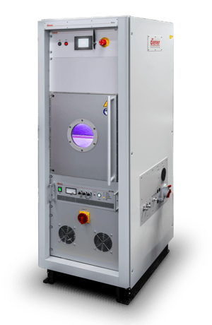 To improve production and product quality, each plasma system is built to the customer’s specific needs, enabling their system to seamlessly fit into their manufacturing process. With over 8,000 plasma systems in the field and a proven track record of success, our plasma technology is unmatched. We maintain a surface applications laboratory to help companies determine objectively how well a plasma treatment addresses their cleaning and etching challenges before they decide to purchase a system.
Other cleaning and etching processes, such as chemical baths and flame treatments can be hazardous for the environment and dangerous for users. Plasma systems are ecologically friendly, minimizing the impact of the environment while improving process and product quality, reliability, and value.
Thierry Plasma has the technology and a system for virtually every commercial, industrial, and scientific plasma treatment need. The efficient and effective plasma cleaning and etching processes made possible by our plasma systems can remove contaminants at the molecular level and provide more precise etching to ensure higher quality manufacturing processes.
To learn more, request a FREE material test study and report, download our eBook “Thierry’s Plasma Surface Modification Solution for Manufacturers."
