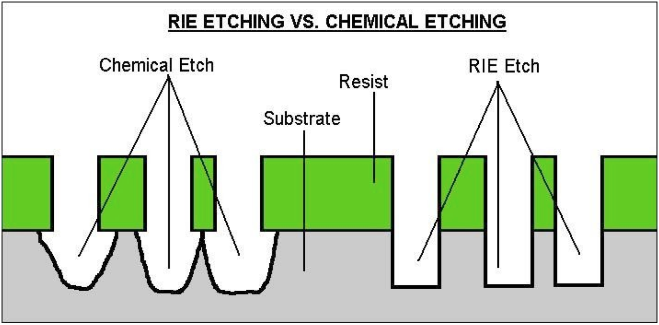
Reactive ion etching (RIE) is a plasma etching process that adds a charge to the part being etched which induces a directional component to the etching process. This directionality of the etch enables significantly smaller etch feature sizes which is commonly used on substrates in the semiconductor industry.
The RIE process is a plasma etching technique that uses a charge to add a directional component to the etching process. This RIE process produces a charge on the part. When this part is charged the etching component of the plasma holds an opposite charge resulting in directional collision of the etch component on the part. The resulting etch is directional enabling much smaller feature size. RIE also enables manufacturers to achieve a faster etch rate than normal etching methods. Since the energy of the ion bombardment onto the surface can be adjusted via electric fields, the etching selectivity can be efficiently controlled.
Deep Reactive Ion Etching (DRIE) is an etching process that was initially developed for etching microelectronic structures with high aspect ratio, e. g. deep trenches on a micrometre scale or even smaller. Nowadays it is also used for the creation of so-called through-silicon vias (TSVs), which is basically an electronic connection through a thin layer of silicon. The production of such structures requires a very anisotropic etching that can only be achieved by such well-directed etching techniques.
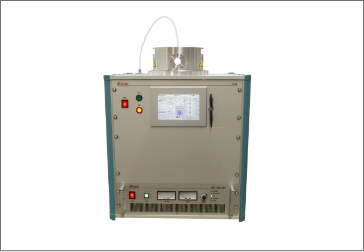
Control Cabinet:
W 560 mm H 560 mm D 420 mm
Chamber:
Ø 3.9 in, L 10.9 in
Chamber Volume:
2
Gas Supply:
1 gas channel via needle valve
Generator:
1 pc. with 40 kHz
(optional: 13.56 MHz or 2.45 GHz)
Control:
Semi-Automatic
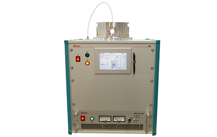
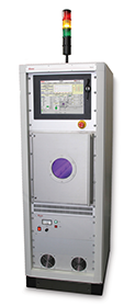
Control Cabinet:
W 600 mm H 1700 mm D 800 mm
Chamber:
Ø 5.9 in, L 12.6 in
Chamber Volume:
5
Gas Supply:
Mass flow controllers
Generator:
1 pc. with 40 kHz
(optional: 13.56 MHz or 2.45 GHz)
Control:
PC
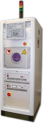
Control Cabinet:
W 600 mm H 1700 mm D 800 mm
Chamber:
W 15.8" x H 15.8" x D 24.6"
Chamber Volume:
100
Gas Supply:
Mass flow controllers
Generator:
1 pc. with 40 kHz
(optional: 13.56 MHz or 2.45 GHz)
Control:
PC