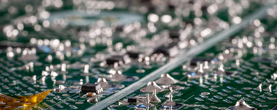
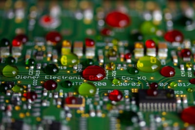
When multilayer printed circuit boards (PCBs) are produced, they utilize base circuit panels manufactured from glass fiber-reinforced epoxy resin. However, when holes are drilled through the various layers to enable electrical connections between them, the friction generated by drilling creates an epoxy smear on the channel walls. This smear must be removed to enable an optimal connection of the layers through a thin coating of copper that is electroplated on the PCB, including the channel walls. If the PCB is not properly cleaned and desmeared, a defect can occur near the plating and inner-layer copper, resulting in poor interconnections. These defects can include open circuits and possibly intermittent defects at higher temperatures, which may cause the circuit ultimately to fail.
 Desmearing involves removing debris from the drill holes, including any epoxy resin that has melted and been dragged over the exposed layers, creating the smear. One method is to use solutions of either potassium permanganate or sodium permanganate to desmear and etch back the drill holes. Another, more effective method, is to use a plasma treatment that can also improve resin coating adhesion by micro-roughening.
To encourage more effective removal of the resin smear, a mixture of gamma-butyrolactone and water is applied to soften the resin. It is then treated with an alkaline permanganate solution that removes the now-pliable resin to create a clean surface. The final step in the process is to neutralize and remove the caustic permanganate residue with an aqueous acidic neutralizer. There are, however, several issues with using permanganate solutions. They require high temperatures to be effective and their caustic nature can be toxic to humans, exposing workers to safety risks and potentially causing a variety of health problems. In addition, a wrong concentration of the solution can result in damage to the PCB polyimide dielectric.
Plasma etching does not require the use of a high-temperature chemical bath like a permanganate solution. Plasma etching is a dry technique that is an environmentally friendly and proven method for thoroughly removing any epoxy resin left behind in the PCB drilling process.
Unlike permanganate solutions which involve wet chemistry and chemicals that become less effective as they age, plasma etching is a highly uniform and inherently cleaner process. It eliminates any toxic wet chemistry waste and its equipment takes up significantly less space on the manufacturing floor. Plasma treatment equipment is even easier to use – once it’s installed and workers familiarized with it, a plasma treatment system does not require highly-skilled personnel to operate it.
To learn more about the benefits of the plasma PCB desmearing process over caustic wet chemistry alternatives, contact the plasma etching experts here at Thierry Corp.
To learn more about plasma etching and its benefits in the electronics manufacturing process, please read our article titled "Plasma Etching and Cleaning Strategy for Better Product Quality."

Comments