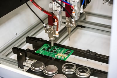
Manufacturers often have issues with their conformal coating bonding to the surface layers of their parts. These issues can be resolved quite easily by treating the parts with a plasma system before the coating. Plasma treatment is a widespread standard instituted in the electronic manufacturing of printed circuit boards (PCBs).
When producing printed circuit boards, plasma activation is a great option to consider. Not only does the plasma activate the surface, but it also cleans the surface of the printed circuit board of any foreign material that may be leftover during production. Most printed circuit board manufacturing processes are aqueous. This creates chemistry that drags on from one manufacturing process step to the next. When employing a plasma activation step, these contaminants are removed with a plasma cleaning before the PCBs proceeds to the subsequent coating process. When a surface is clean, as opposed to having foreign material (FM) on it, the product will have a more uniform coating and stronger bond.
 Printed circuit boards also have many points at which soldering occurs, causing areas to have excess contamination and flux. These contaminants can pose a significant problem when it comes to the conformal coating step. These areas which have excess solder flux are often the areas where the conformal coating bond will fail. A great way to remedy this would be to employ a plasma treatment to clean these areas. Plasma can clean these areas to remove that flux and activate the area where that flux has been removed. This process ensures a clean, activated surface that is ready to take on a coating immediately afterward.
Incorporating plasma activation into a printed circuit board manufacturing line is exceptionally beneficial. The plasma activation treatment will increase the surface energy of the PCB with all the integral parts of the PCB already in place. This will allow the conformal coating to adhere and wet out properly to the surface of the board. Since PCBs have many different elements exposed to them, the surface energy will vary significantly across these elements. Some of these elements will even have very low surface energy, making it very hard to bond a coating to them. A plasma activation will increase the surface energy across all of the exposed elements and provide for a much more uniform coating across the entire printed circuit board.
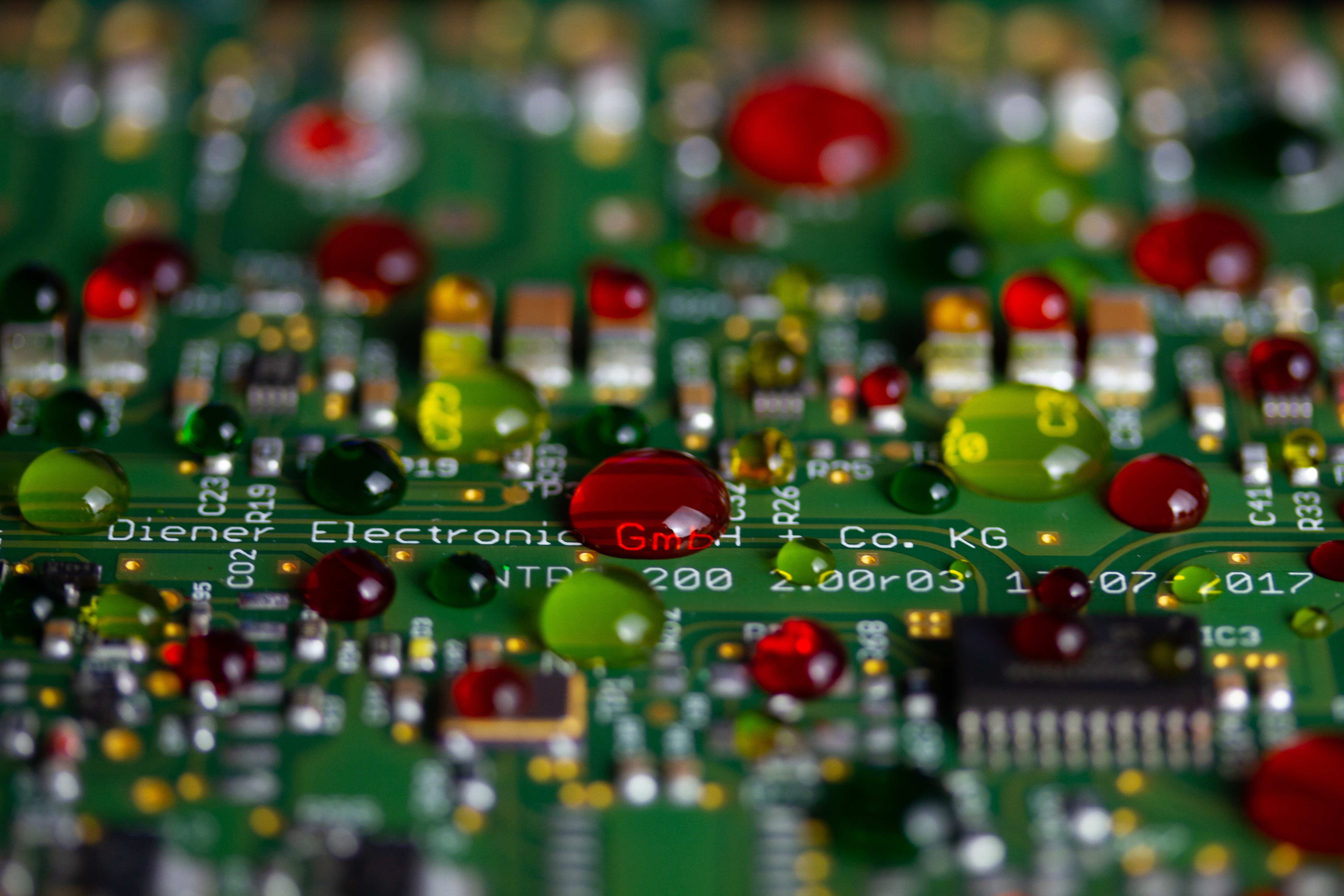
There is often an issue of a conformal coating not adhering to the printed circuit boards without a plasma process. This is because there are problems with the coating wetting out across the board and beading up on the components with low surface energy. When this issue occurs, the entire PCB may have to be scrapped. The resulting waste in the manufacturing process costs the company money. Plasma activation eliminates waste and makes the manufacturing line more profitable.
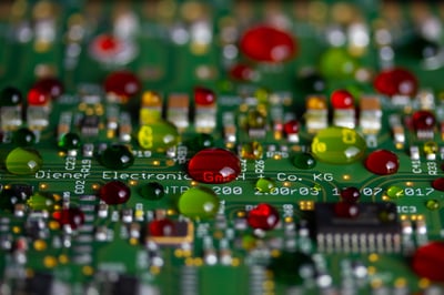 Using plasma activation as a precursor to the bonded coating has many advantages. When applying the coating during the manufacturing process without using plasma, there is a weak bond that occurs. This can allow gaps in the coating where water and other liquids can penetrate and damage the board. When using plasma activation, the new bond performs better than the standard conformal coating and creates a watertight seal where those liquids can't penetrate. This method of improving bond performance makes a better printed circuit board that is not easily damaged.
Integrating plasma cleaning into the manufacturing process can eliminate other steps in the manufacturing line as well. If a plasma cleaning operation is used, the need for a vapor degreaser method can also be eliminated, saving time and money. Solvent-based cleaning solutions can also be eliminated, which could be harmful to the environment. Plasma cleaning is a greener solution than solvents are.
Plasma activation and cleaning are extraordinary processes to implement in a printed circuit board manufacturing line. Plasma activation can improve the surface energy, which creates better adhesion to the surface. Plasma cleaning ensures all contaminants, or foreign material, are removed before the bonding step. Overall, instituting a plasma system in the printed circuit board industry improves the quality of the product, eliminates scrap, and reduces volatile organic compounds (VOCs). It often does these things by replacing a step or multiple steps in a typical manufacturing line, saving time and effort.
To learn more about the benefits of surface activation in the PCB manufacturing process, please read our article titled "Manufacturer’s Surface Activation Guide for Improved Adhesion."
Comments