A very important question in the manufacturing industry is how to remove oxides from components to improve bonding. Plasma etching can enhance the bonding in the electronics industry for better production of printed circuit boards (PCBs) and semiconductors. A plasma treatment will reduce the oxide on the surface and create a clean area to bond after treatment.
 Plasma etching can improve bonding in the electronics industry to produce PCBs and semiconductors more efficiently. Etching away the oxide on the surface creates a pristine surface so that a bonding process can occur effectively. It is vital to have a clean material surface for a bond to adhere properly. Using plasma to reduce the oxide is a very wise choice immediately before a bonding step.
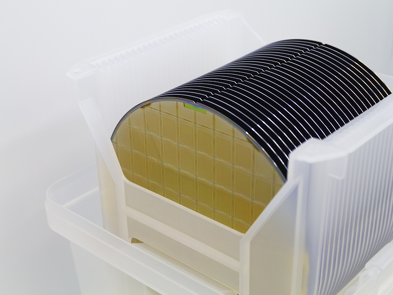
When manufacturers use a ball bonding or wedge bonding process, oxide contamination in the bond nugget leads to material failures in the final bond when producing semiconductors. There is a need to reduce this oxide to have a proper end-product. Using a plasma system to remove the oxide in the lead frame or packaging of die reduces failures and is the most efficient method.
Oxide contamination on a bond can change the impedance of the interconnect and add variability in electronic performance. The problem is that when there is oxide contamination on the surface components, this will create undesired effects that change the intended signal performance of specific components on the PCB or semiconductor. The oxide should be removed, so the specific impedance is achieved.
The most effective process gas for semiconductor manufacturers to use is Hydrogen. Plasma etching with Hydrogen reduces the oxide buildup on the surface of metal components. Hydrogen is the preferred gas for this process because it attacks the oxide which is removed and does not harm the metal once the oxide is removed.
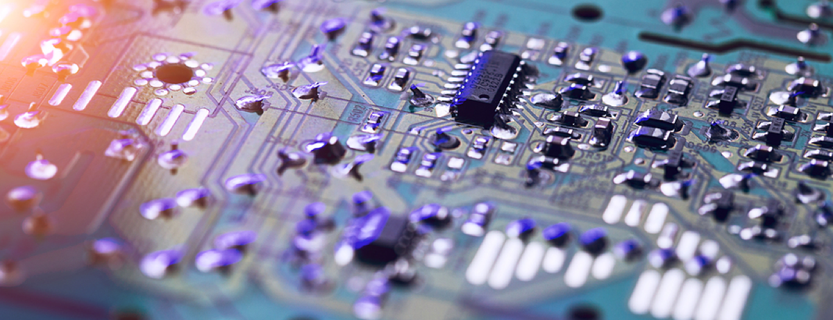
Printed circuit boards, or PCBs, are also manufactured using the plasma etching process. Plasma systems are used to eliminate the contaminants on the PCBs to ensure better solder adhesion performance. Plasma is also used to produce discrete devices and sensors that are frequently used in the automotive and aerospace industries.
Using a source to remove the oxidation that also doesn't damage components is very important. In semiconductor production, a lot of parts can be damaged with Electrostatic discharge (ESD). Plasma will not harm ESD sensitive parts. Hydrogen plasma is commonly used in these processes because all the devices in the chamber experience the same charge, and no differential in electronic potential is observed. This is why plasma is the preferred method to remove oxides from ESD sensitive parts.
Plasma etching is the best way to remove oxides and other contaminants in high volume manufacturing. It is used by many different manufacturers, including automotive, aerospace, semiconductor fabricators, and PCB producers. Hydrogen plasma is the optimal process gas for reducing oxides and enables electronic manufacturers to produce high-volume products efficiently. A plasma etching process can be easily introduced into any manufacturing process to optimize volume and profitability.
To learn more about plasma etching and its benefits in the electronics manufacturing process, please read our article titled "Plasma Etching and Cleaning Strategy for Better Product Quality."

Comments