Manufacturers often ask the question; What would be the best way to remove photoresist from their parts? Plasma ashing or plasma etching is almost always the most efficient and most effective way to do this. It is a better option than other methods, including wet chemistry, which is a more costly process and produces wet chemistry waste.
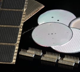
Plasma etching, otherwise known as plasma ashing, is a great way to remove photoresist from printed circuit boards or wafers. It is the most efficient way to remove the photoresist at the foot of the feature. There is usually a small amount of photoresist left at the foot when using chemical methods for removing it. The residual photoresist issue does not occur when using plasma treatment to achieve the same goal. A plasma etching treatment attacks all exposed photoresist on a substrate.
 Vacuum Chamber - When implementing a plasma etching treatment in PCB or wafer production, it is essential to select a vacuum chamber material compatible with your processes. Plasma production in stainless steel chambers can introduce trace levels of metals into the plasma, contaminating the junctions in the manufacturing device. Choosing an aluminum chamber will minimize this sputtering effect further. Ultimately, a quartz chamber would be the best option as this will eliminate any chance of sputtering metal from a chamber onto the PCB or wafer.
Plasma Generator Frequency - A very important aspect of removing photoresist with a plasma system is choosing the correct generator frequency to optimize the etch rate that results from the plasma treatment. The generator frequency can be in a range of the following frequencies; kHz, MHz, and GHz. Many materials can be sensitive to specific frequencies. Ion damage resulting from an incorrect choice in frequency can be very detrimental to the manufacturing process. These details are why it is imperative to know if your device is sensitive to a particular frequency and choose the correct frequency when selecting a plasma source generator.
Plasma Process Gas - Many different types of process gases can be used in the plasma treatment of wafers or PCBs. It is crucial to have a plasma system capable of the proper kind of treatment gas needed for a manufacturer's requirement. Some of these process gases could include oxygen, argon, and helium. If a process needs to have an aggressive etch, fluorine-containing gas is often the choice. The two most popular options are CF4 and SF6. Many processes will also include a multi-step process with a couple of the gases mentioned before as they each have their specific specialty.
Plasma etching to produce PCBs and wafers is a better option than wet chemistry. Wet chemistry is very expensive and produces wet chemistry waste that can be harmful to the people working in the facility and harmful to the environment. Plasma treating wafers and PCBs is cost-effective and extremely efficient. Plasma systems are also very environmentally friendly, where the cost over time is minimal.
Using plasma to etch away photoresist is the best method in the electronics industry today. Plasma systems provide many methods in a manufacturer's toolbox that enable them to customize their process to improve product quality and yield. Other methods, such as wet chemistry, are toxic and harmful to the environment, while plasma can be very clean and environmentally friendly. With the recent movement to provide greener technologies in many fields, plasma technology offers a viable and cost-efficient option to wafer and PCB fabricators.
To learn more about plasma surface cleaning and its benefits in the manufacturing process, please read our article titled "Plasma Etching and Cleaning Strategy for Better Product Quality."


Comments